• 2026.03.30 (Mon)
  • All articles
  • LOGIN
  • JOIN
Global Economic Times
fashionrunwayshow2026
  • Synthesis
  • World
  • Business
  • Industry
  • ICT
  • Distribution Economy
  • Well+Being
  • Travel
  • Eco-News
  • Education
  • Korean Wave News
  • Opinion
  • Arts&Culture
  • Sports
  • People & Life
    • International Student Report
    • With Ambassador
  • Column
    • Cho Kijo Column
    • Cherry Garden Story
    • Ko Yong-chul Column
    • Kim Seul-Ong Column
    • Lee Yeon-sil Column
  • Photo News
  • New Book Guide
MENU
 
Home > Industry

Localization of Specialized Semiconductors Complete: 4-Inch Wafer Yield Hits 95%

KO YONG-CHUL Reporter / Updated : 2026-03-30 08:13:52
  • -
  • +
  • Print


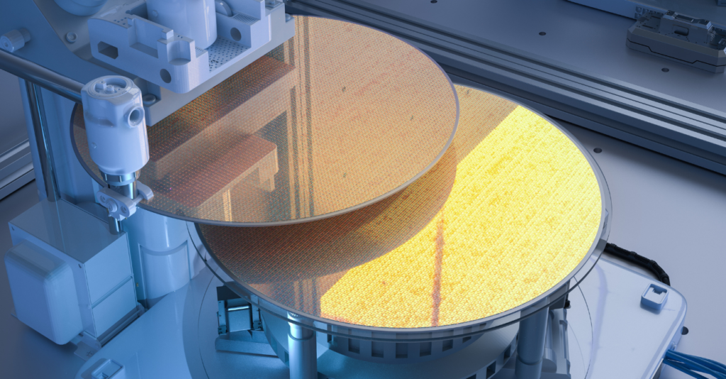
SEOUL — South Korea has secured a critical foothold in the global race for semiconductor sovereignty. The Korea Advanced Nano Fab Center (KANC) announced on March 29, 2026, that it has achieved a breakthrough in the localized production of high-performance compound semiconductor devices—a field previously dominated by total import reliance.

The center confirmed it has reached a 95% yield rate in the manufacturing process for 4-inch Gallium Arsenide (GaAs) metamorphic High Electron Mobility Transistors (mHEMT). This milestone is expected to revolutionize South Korea’s capabilities in defense, aerospace, and next-generation communications.

 
The "Nuclear Core" of Defense Technology
The GaAs mHEMT is a compound semiconductor device created by combining two or more elements. It is widely regarded as the successor to silicon (Si) based semiconductors, overcoming the latter's physical limitations.

Key advantages include:

Superior Speed: Electron mobility is 5 to 6 times faster than that of silicon.
Signal Integrity: It maintains powerful amplification performance in ultra-high frequency bands without signal distortion.
Extreme Durability: It meets rigorous reliability standards required for outer space, where radiation exposure is high, and functions flawlessly in extreme environments.
Due to these traits, the device is often called the "nuclear core of defense semiconductors." It is an essential component for Advanced Electronically Scanned Array (AESA) radars and missile seekers used in cutting-edge weaponry.

 
Breaking the Scaling Barrier
Historically, Gallium Arsenide has been notoriously difficult to handle due to its brittle nature compared to silicon. Consequently, production was largely limited to small-scale 2 or 3-inch wafers. Despite South Korea's strong design capabilities, a lack of domestic manufacturing infrastructure meant that over 90% of these core components had to be imported from overseas.

By transitioning from the traditional 2-3 inch scale to a 4-inch large-area wafer while maintaining a 95% yield, KANC has effectively bridged the gap between research and mass production. This achievement significantly enhances both production efficiency and quality control.

 
Building a Self-Sustaining Ecosystem
KANC is now shifting its focus toward fostering a domestic "fabless" ecosystem. The center has begun developing a Process Design Kit (PDK)—a digital toolkit containing physical characterization data of the manufacturing process. Once this platform is finalized, domestic fabless companies will be able to design complex, high-performance chips using KANC’s 4-inch process for local mass production.

Furthermore, the center will provide Multi-Project Wafer (MPW) support. MPW allows multiple companies to share a single wafer for their designs, drastically reducing the prototype costs for small-to-medium-sized enterprises (SMEs), which can otherwise reach hundreds of millions of won per wafer.

"The 4-inch wafer process will be a turning point in lowering production costs and accelerating supply speeds," said an industry official. "A 95% yield indicates that the process has reached a level of stability suitable for actual commercialization and mass production, moving far beyond the simple R&D stage."
By resolving the long-standing issues of high costs and extended waiting times associated with overseas foundries, this localization effort is set to become the primary engine driving the autonomy of South Korea’s compound semiconductor industry.

[Copyright (c) Global Economic Times. All Rights Reserved.]

  • #globaleconomictimes
  • #micorea
  • #mykorea
  • #nammidonganews
  • #singaporenewsk
  • #Samsung
  • #Daewoo
  • #Hyosung
  • #Apple
  • #korea
KO YONG-CHUL Reporter
Reporter Page

Popular articles

  • Ko Sang-goo, President of World Federation of Korean Associations, Elected as First Private Sector Chair of World Korean Community Leaders Convention

  • The "Invisible Violence" on Japanese Streets: The Rise of 'Butsukari'

  • Hunminjeongeum Liaodong Academic Expedition Issues Letters to Leaders of Korea and China at Shenyang Consulate

I like it
Share
  • Facebook
  • X
  • Kakaotalk
  • LINE
  • BAND
  • NAVER
  • https://globaleconomictimes.kr/article/1065568251631815 Copy URL copied.
Comments >

Comments 0

Weekly Hot Issue

  • Com2uS Pro Baseball 2026 Hits a Home Run with Massive Update for KBO Opening Day
  • Icheon City Expands AI Robot Companion Program to Combat Senior Isolation and Enhance Safety
  • Generative AI Enters the Classroom: GBSA Appoints 130 Specialized Instructors to Lead Gyeonggi’s Digital Future
  • "AI Won't Replace Security, It Will Fuel It": Cyber Security Market Set to Double
  • “Urban Community Headquarters Holds 1st Sustainable Urban Community Forum in Sejong”
  • Cheonan City Empowers Citizens to Validate Smart City Services: "Reverse-Proposing Solutions to User Inconvenience"

Most Viewed

1
The Zenith of ‘K-Strawberries’: A Sweet Innovation Unfolds in Nonsan… The 28th Nonsan Strawberry Festival Opens
2
Netanyahu Declares Decisive Blow to Iran’s Nuclear and Missile Programs, Signals Early End to War
3
K-Beauty SMEs Join Forces with Distributors: A New Paradigm for Global Expansion through Strategic Consortiums
4
Global Food Delivery Giants Hit Record Highs: Subscription and Quick-Commerce Emerge as Key Growth Engines
5
Won Breaches 1,500 Mark for First Time Since Financial Crisis; KOSPI Stabilizes at 5,500 Amid Chip Rally
광고문의
임시1
임시3
임시2

Hot Issue

Samsung Completes Transition to 236-Layer 8th Gen V-NAND in Xi’an; 9th Gen Mass Production Slated for Late 2026

LG Electronics Leverages 'Physical AI' to Transform Logistics into a Smart Factory Frontier

Localization of Specialized Semiconductors Complete: 4-Inch Wafer Yield Hits 95%

Samsung and LG Clash in Milan Over European HVAC Supremacy at MCE 2026

Let’s recycle the old blankets in Jeju Island’s closet instead of incinerating them.

Global Economic Times
korocamia@naver.com
CEO : LEE YEON-SIL
Publisher : KO YONG-CHUL
Registration number : Seoul, A55681
Registration Date : 2024-10-24
Youth Protection Manager: KO YONG-CHUL
Singapore Headquarters
5A Woodlands Road #11-34 The Tennery. S'677728
Korean Branch
Phone : +82(0)10 4724 5264
#304, 6 Nonhyeon-ro 111-gil, Gangnam-gu, Seoul
Copyright © Global Economic Times All Rights Reserved
  • 에이펙2025
  • APEC2025가이드북TV
  • 독도는우리땅
Search
Category
  • All articles
  • Synthesis
  • World
  • Business
  • Industry
  • ICT
  • Distribution Economy
  • Well+Being
  • Travel
  • Eco-News
  • Education
  • Korean Wave News
  • Opinion
  • Arts&Culture
  • Sports
  • People & Life 
    • 전체
    • International Student Report
    • With Ambassador
  • Column 
    • 전체
    • Cho Kijo Column
    • Cherry Garden Story
    • Ko Yong-chul Column
    • Kim Seul-Ong Column
    • Lee Yeon-sil Column
  • Photo News
  • New Book Guide
  • Multicultural News
  • Jobs & Workers