• 2026.06.05 (Fri)
  • All articles
  • LOGIN
  • JOIN
Global Economic Times
fashionrunwayshow2026
  • Synthesis
  • World
  • Business
  • Industry
  • ICT
  • Distribution Economy
  • Well+Being
  • Travel
  • Eco-News
  • Education
  • Korean Wave News
  • Opinion
  • Arts&Culture
  • Sports
  • People & Life
    • International Student Report
    • With Ambassador
  • Column
    • Cho Kijo Column
    • Cherry Garden Story
    • Ko Yong-chul Column
    • Kim Seul-Ong Column
    • Lee Yeon-sil Column
  • Photo News
  • New Book Guide
MENU
 
Home > Industry

Samsung’s Taylor Fab Enters "Setup Mode": 3,000 Global Engineers Converge on Texas

Graciela Maria Reporter / Updated : 2026-04-02 05:18:48
  • -
  • +
  • Print


(C) WCCFTech


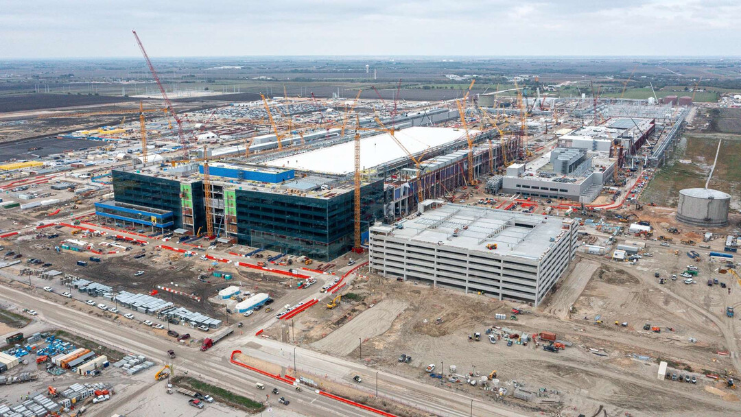
Samsung Electronics has officially transitioned from the construction phase to the critical "setup" phase—the installation and trial operation of semiconductor equipment—at its massive foundry site in Taylor, Texas. As the tech giant races to secure North American Big Tech clients for its 2nm process, a "global coalition" of over 3,000 engineers is descending upon the site at 1530 FM 973, Taylor, TX.

From Concrete to Core Technology
According to industry sources on April 1, Samsung has posted 178 job openings across 146 core sectors, including field technicians, operations management, infrastructure, and safety. This massive hiring wave signals that the facility has reached the "Ramp-up" stage, where machines are moved into the cleanrooms and calibrated for mass production.

More than half of the recruitment focus is on specialized personnel capable of handling 2-nanometer (2nm) cutting-edge nodes. Currently, the global talent pool with experience in sub-3nm mass production is limited to a handful of experts from Samsung (South Korea), TSMC (Taiwan), and Intel (USA). Samsung’s strategy involves not only hiring local Texan talent but also relocating personnel from its Austin campus and absorbing researchers from labs worldwide.

The 3,000-Strong Engineer Coalition
The "Setup" phase is a collaborative effort between Samsung and the world’s leading semiconductor equipment manufacturers.

Samsung Direct Hires: Approximately 1,500 personnel.
Equipment Partners: At least 1,500 expert engineers from global top-tier firms like ASML (EUV lithography from the Netherlands), Lam Research (Etching from the US), and KLA (Inspection/Measurement from the US).
Industry standards suggest that a single piece of advanced equipment requires up to 10 engineers for installation and testing. Given that hundreds of precision machines—with a total weight estimated at 20,000 tons—are being moved into the Taylor fab, the scale of human capital required is unprecedented. Roughly 5,000 tons of equipment are being shipped from Korea, while another 6,000 tons are arriving from European and Japanese production bases.

A City Reborn: The "Samsung Effect"
The Taylor Fab 1 has already obtained Temporary Certificate of Occupancy (TCO) for major zones. Last month, it reportedly began trial runs for core equipment, including Extreme Ultraviolet (EUV) lithography scanners.

When factoring in Samsung’s direct employees, equipment partner engineers, infrastructure contractors, and remaining construction crews, the total headcount at the site is expected to reach 10,000. To put this in perspective, this "semiconductor army" represents more than half of the entire population of Taylor (approx. 18,000).

"For deposition equipment alone, we may see dozens to hundreds of units being installed. When you combine the staff from various suppliers, we are seeing a demand for nearly 1,000 setup personnel per month," said an industry official. "When you add safety inspectors, facility engineers, and support staff, the site is effectively becoming a self-contained tech city."

The Roadmap to 2nm Dominance
The primary objective of the Taylor site is to establish a North American stronghold for 2nm foundry services. By producing locally, Samsung aims to gain a competitive edge in securing contracts from US-based AI and Big Tech firms that require low-latency supply chains and cutting-edge silicon.

The Taylor fab targets an initial production capacity of 50,000 wafers per month (WSPM). Following the current trial operations and equipment calibration through the end of 2026, the facility is projected to commence full-scale mass production by 2027, marking a new chapter in the global semiconductor race.

[Copyright (c) Global Economic Times. All Rights Reserved.]

  • #globaleconomictimes
  • #micorea
  • #mykorea
  • #nammidonganews
  • #singaporenewsk
  • #Samsung
  • #Daewoo
  • #Hyosung
  • #Apple
  • #korea
Graciela Maria Reporter

Popular articles

  • Alleged Marital Rift Between Macrons Tied to Iranian Actress: New Claims Emerge

  • OpenAI Redefines Human-AI Interaction with ‘GPT-Realtime-2’ and New Suite of Live Voice Models

  • Taiwanese President Lai Ching-te Honors Japanese Engineer from Colonial Era: "We Are Family"

I like it
Share
  • Facebook
  • X
  • Kakaotalk
  • LINE
  • BAND
  • NAVER
  • https://globaleconomictimes.kr/article/1065557836546118 Copy URL copied.
Comments >

Comments 0

Weekly Hot Issue

  • Samsung Electronics Super-Enterprise Union Loses Majority Status Amid Backlash Over Bonus Disparities
  • Samsung to Embed Vital Signs and Heart Health Scores in Upcoming Galaxy Watch9 Lineup
  • Apple Honors Digital Excellence: 12 Exceptional Apps and Games Celebrated at the 2026 Design Awards
  • Nexon Revamps Signature Youth Coding Competition into AI-Driven 'Nexon Young Programmers Cup'
  • Tech University of Korea Gathers 200 Game and AI Researchers to Discuss Industrial Expansion
  • Major Korean Telcos Trim Online-Exclusive Plans by Up to 50% Amid Shift to Unified Mobile Tariffs

Most Viewed

1
From a moment of collective sacrifice to a moment of collective democracy: The Timing of the Election in Ethiopia and Korea
2
U.S. Holds Off on Immediate Comprehensive Semiconductor Tariffs, but Pressure Mounts for Samsung and SK Hynix to Accelerate Domestic Investments
3
[Interview] "Halal is Not a Religious Regulation, but a 'Trust Infrastructure'… Creating a Premium 'K-Halal' Centered on Data and Platforms"
4
‘600 Million Won Bonus’ at Samsung Electronics Triggers Deep Sense of Relative Deprivation Among Korean Workers
5
Bomb Attack Targets Moving Train in Pakistan: At Least 29 Dead, 102 Injured
광고문의
임시1
임시3
임시2

Hot Issue

Murata Unveils Next-Gen Resin Electrode MLCC for Automotive Applications

Samsung to Embed Vital Signs and Heart Health Scores in Upcoming Galaxy Watch9 Lineup

L&F Plus Secures KRW 220 Billion from National Growth Fund to Anchor South Korea’s First Mass LFP Cathode Production

Samsung Electronics Super-Enterprise Union Loses Majority Status Amid Backlash Over Bonus Disparities

Fashion Runway Show 2026

Global Economic Times
korocamia@naver.com
CEO : LEE YEON-SIL
Publisher : KO YONG-CHUL
Registration number : Seoul, A55681
Registration Date : 2024-10-24
Youth Protection Manager: KO YONG-CHUL
Singapore Headquarters
5A Woodlands Road #11-34 The Tennery. S'677728
Korean Branch
Phone : +82(0)10 4724 5264
#304, 6 Nonhyeon-ro 111-gil, Gangnam-gu, Seoul
Copyright © Global Economic Times All Rights Reserved
  • 에이펙2025
  • APEC2025가이드북TV
  • 반달곰 프로젝트
Search
Category
  • All articles
  • Synthesis
  • World
  • Business
  • Industry
  • ICT
  • Distribution Economy
  • Well+Being
  • Travel
  • Eco-News
  • Education
  • Korean Wave News
  • Opinion
  • Arts&Culture
  • Sports
  • People & Life 
    • 전체
    • International Student Report
    • With Ambassador
  • Column 
    • 전체
    • Cho Kijo Column
    • Cherry Garden Story
    • Ko Yong-chul Column
    • Kim Seul-Ong Column
    • Lee Yeon-sil Column
  • Photo News
  • New Book Guide
  • Multicultural News
  • Jobs & Workers