


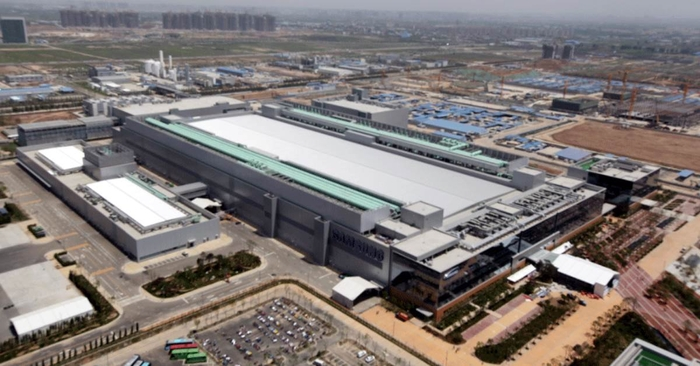
XI'AN, China — In a strategic move to solidify its dominance in the global memory market, Samsung Electronics has officially completed the first phase of its advanced process migration at its NAND flash production complex in Xi’an, China. The facility has successfully transitioned from legacy 128-layer (V6) production to mass-producing high-performance 236-layer 8th Generation V-NAND (V8), signaling a new era for the company’s most critical overseas manufacturing hub.
According to industry sources on March 29, the Xi’an plant has finalized the equipment overhauls and optimization required for V8 production. Furthermore, Samsung is accelerating plans to deploy its cutting-edge 286-layer 9th Generation (V9) NAND within the same complex before the end of the year, ensuring the facility remains at the forefront of the artificial intelligence (AI) infrastructure boom.
A Strategic Pivot Toward High-Density Storage
The transition marks a definitive end to the 128-layer era at the Xi’an site. In the world of NAND flash, "layers" refer to the vertical stacking of memory cells; higher stack counts directly translate to higher data density and improved power efficiency.
Samsung’s decision to phase out the 6th Generation V-NAND stems from a shifting market landscape where legacy products are no longer sufficient to maintain a competitive edge. The move is driven by three primary catalysts:
The Rise of Enterprise SSDs (eSSD): The explosion of AI server investments has created an insatiable demand for high-capacity storage. Enterprise clients are increasingly seeking V8 and V9 solutions to handle the massive datasets required for LLM (Large Language Model) training.
Narrowing Technological Gaps: Regional competitors, most notably China’s YMTC, have reportedly achieved mass production of 294-layer NAND. By upgrading Xi'an—which accounts for approximately 40% of Samsung’s total NAND output—Samsung is re-establishing a clear "technological gap" to prevent market share erosion.
Geopolitical Resilience: Amid ongoing U.S.-China trade tensions, Samsung has utilized its "Validated End-User" (VEU) status to import necessary lithography and etching equipment. However, with the regulatory environment requiring annual renewals, Samsung is moving swiftly to install advanced nodes while the window of stability remains open.
The Roadmap: From V8 to the 400-Layer Frontier
The Xi’an complex consists of two major production lines. While the first phase focused on bringing the 8th Gen V-NAND online, the second plant (X2) is currently being primed for the 9th Generation (V9).
The V9 NAND represents Samsung’s most sophisticated current architecture, featuring industry-leading bit density. With the Xi’an facility handling the bulk of V8 and V9 volume, Samsung’s domestic plants in Pyeongtaek, South Korea, are expected to shift their focus toward the next frontier: 10th Generation (V10) V-NAND.
"The establishment of a stable V8 and V9 production base in China allows our Korean operations to aggressively pursue the V10, which is estimated to exceed 400 layers," noted an industry analyst. "This 'two-track' strategy ensures volume stability in China while pushing the R&D envelope in Korea."
Market Outlook and Implications
The completion of this transition is expected to significantly improve Samsung's margins in the memory division. By shrinking the die size through higher layering, Samsung can produce more bits per wafer, effectively lowering the cost per gigabyte.
While Samsung officially maintains a cautious stance—stating that "specific production schedules cannot be confirmed"—the company reiterated its commitment to a "leading-edge-first" portfolio. As GIGABYTE and other infrastructure providers showcase AI-driven telecommunications at events like MWC 2026, the need for the very chips produced in Xi’an has never been higher.
With the 9th Generation transition expected to be operational by Q4 2026, Samsung is positioned to dominate the premium eSSD market, providing the backbone for the next generation of global AI data centers.
[Copyright (c) Global Economic Times. All Rights Reserved.]