


Samsung Electronics has expanded its local footprint by acquiring an additional building near the headquarters of its American semiconductor subsidiary in Silicon Valley. This move is interpreted as a strategic step to strengthen custom semiconductor collaborations with big tech giants such as Nvidia and Google.
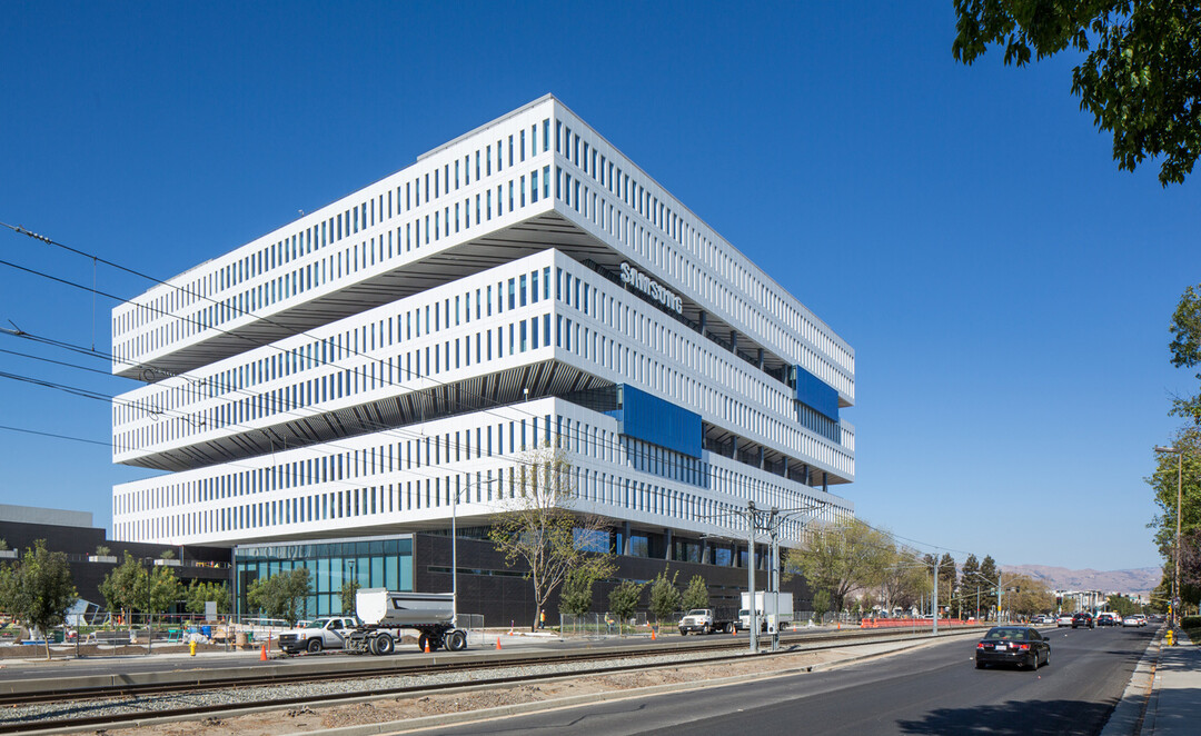
According to Santa Clara County on the 25th, Samsung Electronics purchased a building near its Americas headquarters in San Jose for $29.5 million (approx. 40 billion won) in all cash on the 15th. With this latest acquisition, a campus-style layout has been established, connecting the new building side-by-side with the existing 10-story headquarters and another building purchased from Apple in February of last year.
The total site area of the two buildings acquired over the past year and this year is approximately 40,000 square meters. Combined with the existing headquarters site of roughly 38,400 square meters, Samsung's total secured land area reaches about 78,400 square meters—roughly double the size of its original headquarters property.
Built in 1985, the newly acquired single-story R&D and office facility can accommodate 250 to 300 people. Recently, the US subsidiary of YC, a semiconductor testing equipment partner of Samsung Electronics, was registered at this location. The facility is also well-equipped for semiconductor research and development, featuring a high ceiling of approximately 5.5 meters—higher than general office buildings—along with a 4,000-ampere switchboard and a 1,000kVA transformer. However, Samsung plans to initially utilize the space for offices rather than immediate research facilities.
This site expansion is closely intertwined with Samsung's custom memory business initiatives. In August, at the semiconductor academic conference "Hot Chips 2026" held at Stanford University in the US, Samsung unveiled its development direction for customer-tailored High Bandwidth Memory (HBM). The core strategy involves integrating custom features, such as memory control circuitry, directly into the base die at the very bottom of the HBM. Achieving this requires close cooperation with big tech companies from the AI accelerator development stage to reflect individual customer requirements.
Samsung’s push to expand its local workforce in Silicon Valley is seen as part of this broader strategic vision.
[Copyright (c) Global Economic Times. All Rights Reserved.]